Creating professional-quality double-sided PCBs at home is a challenging but rewarding process. In this guide, we will walk you through a hybrid workflow using the Snapmaker’s Laser and CNC modules. By combining laser ablation for trace isolation and CNC milling for drilling, you can achieve high-precision prototypes.
This guide is intended for advanced hobbyists and engineers using the Snapmaker Laser + CNC modules who want reliable double-sided PCB prototypes without professional fabrication.
You can check our Instagram video here: Solar Team Solaris – Snapmaker 3-in-1 | Double Sided PCB Shorts
Table of Contents
- Credits & Prerequisites
- Tested Devices & Hardware Compatibility
- General Safety & Etching Warnings
- Step 1: Material Preparation
- Step 2: Circuit Design & Export
- Step 3: FlatCAM Processing
- Step 4: Mirroring the Bottom Layer
- Step 5: Generating Laser G-Code (Isolation)
- Step 6: Preparing the Front and Bottom Copper Gcodes for the Laser Engraving
- Step 7: PCB Cutout and Drilling-Milling Design
- Step 8: Drilling and Milling
- Step 9: Laser Ablation on the Snapmaker
- Step 10: Chemical Etching
- Step 11: Paint Removal
- Step 12: CNC Drilling & Alignment
- Step 13: The PCB Mask and Laser Processing
- Step 14: Cutting and Finishing
- Final Result
Credits & Prerequisites
A huge thanks to Ozan Karaca for the UART to CAN-Bus design used in this walkthrough. We also want to express our gratitude to Snapmaker for their generous sponsorship and for providing the hybrid 3-in-1 manufacturing ecosystem that makes this kind of rapid, high-precision prototyping possible for our team.
Before diving in, make sure you have the following hardware, software, and safety gear ready to go:
Hardware & Consumables:
- Standard double-sided copper-clad board
- Fawori black matte acrylic spray paint
- Ferric Chloride (FeCl3) etchant
- Polyester resin cleaner solvent or Isopropyl Alcohol (IPA)
- High-grit sandpaper
- Green UV solder mask
- Double-sided tape
- Snapmaker CNC Bits: 1.5mm flat end mill, 0.5mm drill bit, 3.2mm flat end mill
Software:
- KiCad (for circuit design and Gerber export)
- Gerbv (gEDA’s Gerber Viewer)
- FlatCAM version 8.994 (for toolpath generation). To download the same version of it, click here.
Tested Devices & Hardware Compatibility
This specific guide and the parameters shown in the screenshots were developed and tested using the Snapmaker Artisan Premium equipped with the 40W Laser Module and the standard CNC module.
However, this workflow is highly adaptable. We have successfully used and we are repeatedly using this exact process on the Snapmaker 2.0 equipped with the 10W Laser Module.
Note for 10W/20W Users: If you are following along with a lower-wattage laser module, remember that you will need to scale your laser power settings (or adjust your passes/feedrate) accordingly during the ablation steps to ensure the black paint is fully removed.
General Safety & Etching Warnings
Safety First
This workflow utilizes highly corrosive chemicals and powerful laser ablation. Always operate the Snapmaker within its protective enclosure to shield your eyes from scattered laser radiation and to properly vent the toxic fumes generated when burning away the acrylic paint.
Chemical Handling Warning
Ferric Chloride is highly corrosive and will stain skin, clothes, and surfaces permanently. Always wear nitrile gloves and safety goggles during this step. Perform the etching in a well-ventilated area. Never pour used Ferric Chloride down the sink, as it will destroy your plumbing; store it in a sealed, clearly labeled plastic container and take it to a hazardous waste disposal facility.
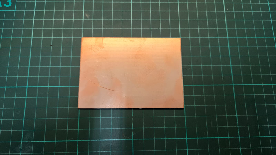
Step 1: Material Preparation
To begin with, source a standard double-sided copper-clad board. You will also need a can of black matte acrylic spray paint:
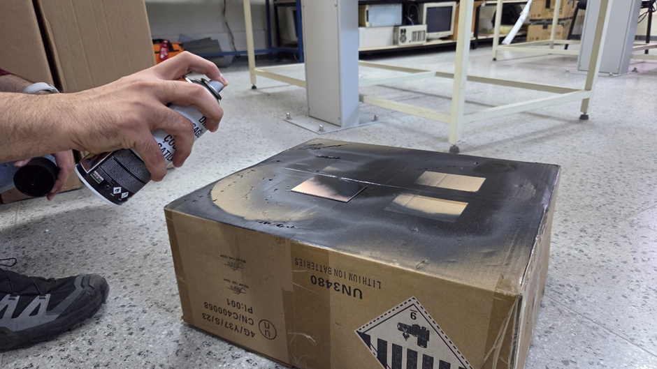
Next, apply two even coats of matte acrylic spray to both sides of the PCB. Ensure the paint is fully dried before proceeding; this layer will act as our etch resist during the laser process.

Then, apply two even coats of the matte acrylic spray to both sides of the PCB. Ensure the paint is fully dried before proceeding; this layer will act as our etch resist during the laser process:
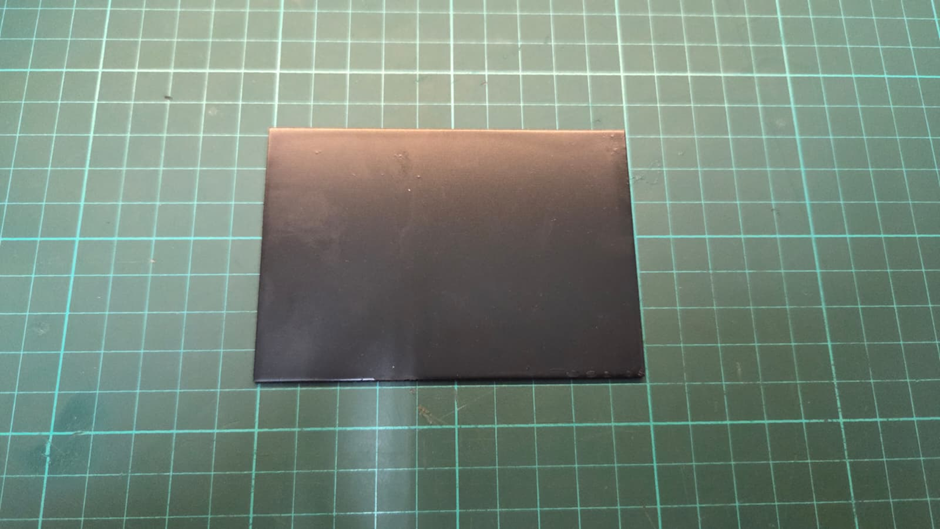
Hence the result, fully dried PCB:
Step 2: Circuit Design & Export
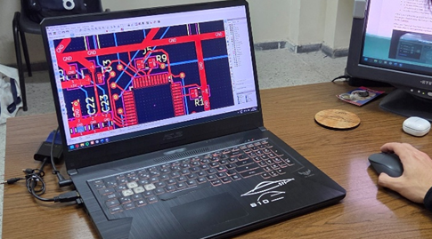
First, we designed our circuit schematic and layout using KiCad:

Next, Kicad layout design:
For this workflow, we recommend the following design rules to ensure compatibility with standard CNC bits:
- Minimum Trace Width: 0.254 mm
- Clearance/Spacing: 0.2 mm
- Via Diameter: 0.5 mm
Exporting Files
When exporting your Gerbers, use the standard manufacturing settings:

Exported files are:

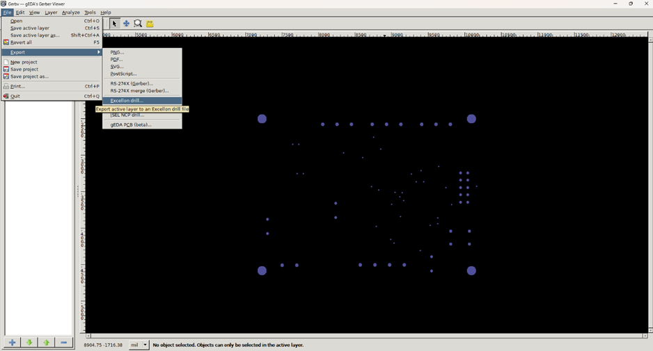
CRITICAL STEP: The default KiCad Excellon drill file format may not import correctly into FlatCAM. You must open your KiCad Excellon (.drl) file in Gerbv first, and then immediately re-export it. If FlatCAM crashes later during the milling setup, it is usually because this step was skipped.
Export option in the GerbV program:
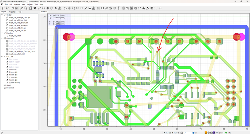
Step 3: FlatCAM Processing
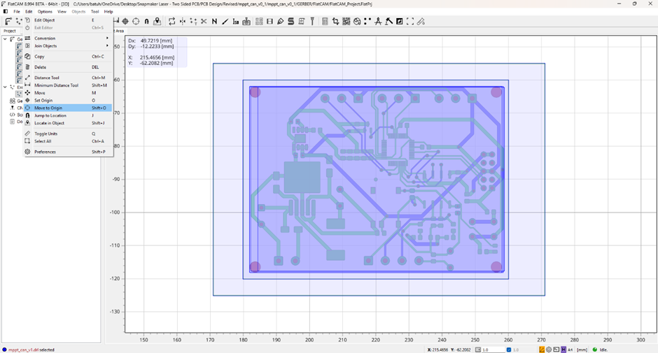
In FlatCAM, switch the interface from “Basic” to “Advanced” in the preferences menu to access full control. Import all your Gerber layers and the re-exported Excellon drill file:

Draw a rectangle around your PCB design to define the board dimensions (For our PCB board, 100mm x 70mm). This boundary is crucial as it serves as the reference axis for mirroring the bottom layer later. (You need to do this with your PCB design software.)

Setting the Boundary Area
Of course, we add our new gerber file to the FlatCAM project. We select everything then move to the origin under the “Edit” tab:
Step 4: Mirroring the Bottom Layer
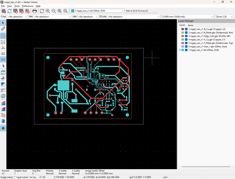
We have the normal Gerber View of the design as:
Open the 2-Sided PCB Tool in FlatCAM. Set the bottom copper Gerber file as the Source Object. Next, select the boundary rectangle on the canvas to define your reference area and click the Calculate Bounds Values button. Once the coordinates are set, choose the Y-axis and click Mirror Object to flip the design horizontally. This ensures the bottom traces align correctly when you flip the physical board.

The result of the Y-axis mirror operation, showing the bottom layer flipped relative to the frame:
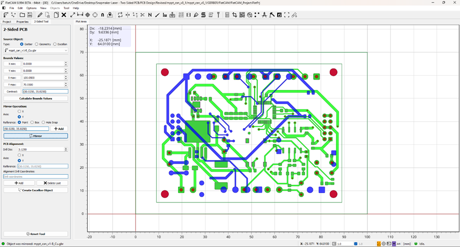
Now we mirror the back mask by choosing the back mask gerber file in the “source object” section of the tool and mirror as given below:

Step 5: Generating Laser G-Code (Isolation)
All laser parameters in this guide are based on the Snapmaker 40W laser module. Users of 10W or 20W modules must scale power accordingly.
Top (Front) Copper
We double click the top/front copper gerber under the “Project” tab to choose the “Isolation Routing” tool:
- Bit size of 0.15 mm, 15% of overlap with 12 passes in isolation tool, TT: C1,

Now we open the geometry object just created by the isolation routing tool:
- C1 tool type in isolation tool,
- 0.15 mm of bit size, C1 tool type, offset is path with type “Iso”, 10% of laser power, 700 mm/min of federate X-Y, GRBL Laser as the preprocessor,

We will save the file as .nc file for the machine. The resulting plotting:

We simply repeat the same for the bottom copper gerber file. Here is the bottom copper and front copper plotting:

We disable plots for CNC job and geometries for front and back copper sides to make it easier for us to follow.
Now we prepare the masks for the front and bottom gerber files.
- We double click the front mask and then open the Paint tool,
- We set the tool diameter to 0.15 and tool type to C1,
- Overlap is 15%.
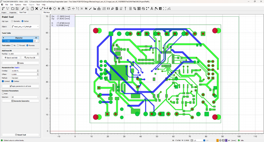
And we perform the same steps for the back mask gerber as well.
With the geometries generated for the masks front and back, we can now double click them to set the laser engraving settings, same as before:
- C1 tool type in isolation tool,
- 0.15 mm of bit size, C1 tool type, offset is path with type “Iso”, 10% of laser power, 700 mm/min of federate X-Y, GRBL Laser as the preprocessor,

Then we save the Gcodes.
Step 6: Preparing the Front and Bottom Copper Gcodes for the Laser Engraving
First, we repeat the gcode, for 5 times in the same file as:
From

Until

Copied and pasted 5 more times to repeat continuously:

Then we repeat the same process for the bottom gcode as well.
We repeat the same process to obtain 5 times repeated code for the mask gcodes as well.
Step 7: PCB Cutout and Drilling-Milling Design
Cutout
We double click to open the edge cut gerber file. Then we open the “cutout tool”. We are going to use the Snapmaker 1.5mm bit for this purpose, therefore our settings are:
- Tool dia: 1.5mm,
- Cut z: -1.9,
- No multidepth,
- Margin: 0
- Gaps: none.

We double click to open the geometry and apply the following settings:
- Preprocessor: Marlin,
- Tool diameter: Enter for the bit,
- Tool type: Enter for the bit,
- Cut Z: -2,
- Feedrate X-Y and Z: 60,
- Spindle speed: 18000.

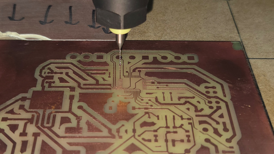
Step 8: Drilling and Milling
Vias
We designed vias to be 0.5mm so we will use a suitable 0.5mm bit. With the following settings:

Settings are as follows:
- Preprocessor: Marlin,
- Cut Z: -2,
- Feedrate Z: 120,
- Spindle speed: 18000.
We open the Excellon file that contains all the vias to be drilled or milled and choose only 0.5mm one. Then we choose the Drilling Tool, then we apply the settings as:

Drilling the Holes
We repeat the same procedure for drilling. For our case, we will drill 0.5mm, 0.99 mm – 1.09 mm(~1mm) and 1.29mm (~1.3mm) with drilling.
Milling the Bigger Holes
For 3.2mm we will use the Flat End Mill (double cut 1.5) bit to perform milling. First, we select the 3.2mm diameter from the table:
- Under “Utilities” we fill the bit size as 1.5000 and click Mill Drills,

If the FlatCAM crashes, you need to export the DRL file using GerbV program, as previously explained using GerbV.
- Preprocessor: Marlin,
- Tool diameter: Enter for the bit,
- Tool type: Enter for the bit,
- Cut Z: -2,
- Feedrate X-Y and Z: 60,
- Spindle speed: 18000.

Finally, we have the following list of objects under the Project tab with the plot given,

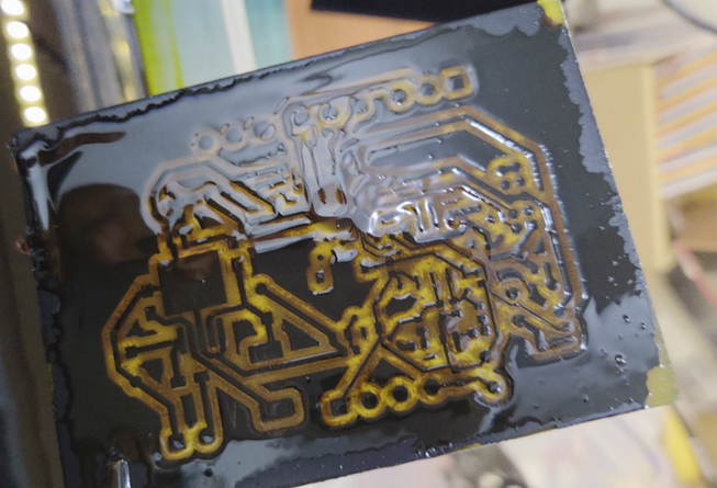
Step 9: Laser Ablation on the Snapmaker
To maintain perfect alignment between the top and bottom sides, attach a sacrificial material to the bed to act as a physical “fence” or anchor. We used an old PCB and Snapmaker CNC to carve out a corner. One can also use the laser module to cut a template out of wood.

We are using the CNC table for the laser engraving as well. Because we will be also using the CNC module and it will be easier to set the same work coordinates for X-Y axes:

We use double sided tape to fix the PCB to its place. Our PCB has 1.5mm thickness.
Workflow
To maintain perfect alignment between the top and bottom sides, you must attach a sacrificial material to the bed to act as a physical “fence” or anchor. We carved out a corner of an old PCB using the CNC module. Do not move this anchor plate until the entire project is finished.
- Ablate Top Copper paint,
- Flip the board horizontally,
- Ablate Bottom Copper paint.
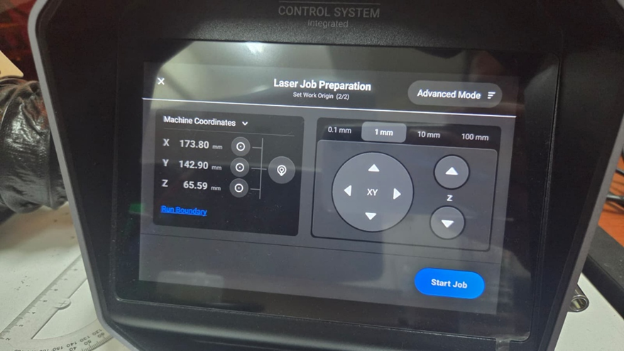
Crucial: Record your machine coordinates for the Work Origin so you can return to them exactly if the machine restarts or modules are swapped:
And here is the laser spot for marking the origin, side view for front copper:

We have the front copper’s result as,

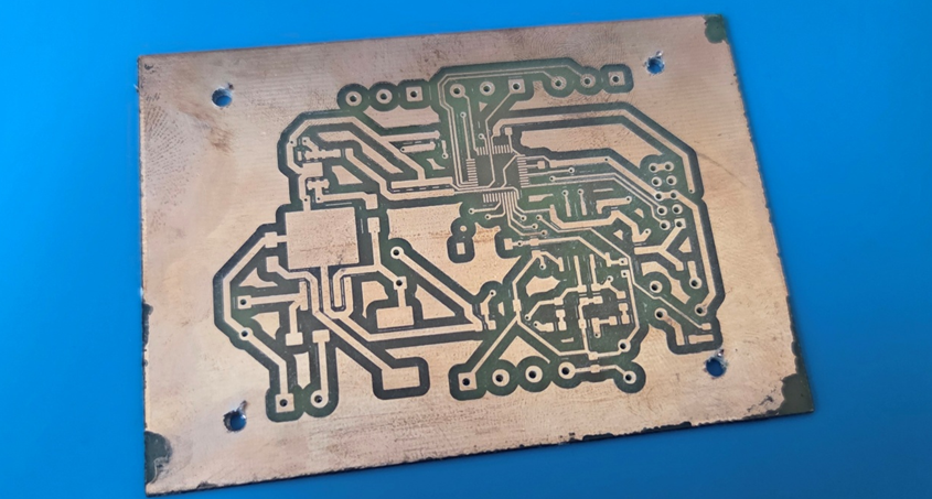
Step 10: Chemical Etching
The Etchant
Our etchant is FeCl3 (Ferric chloride).
Process
Submerge the board in a Ferric Chloride (FeCl3) solution. Gently agitate the container to speed up the reaction. The paint remaining on the board will protect the traces while the exposed copper is dissolved. (Heating up the solution beforehand is a very good option as well.):
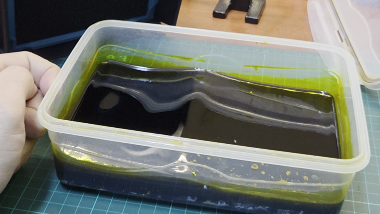
Monitor the process closely. Remove the board as soon as the unwanted copper is gone to prevent “over-etching,” which can damage your traces:
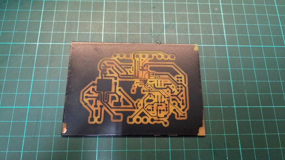
Result of Etching
Front copper:
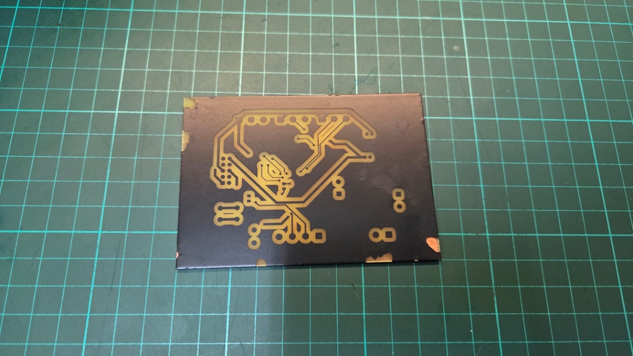
Bottom copper:
Now we can continue with removing the black paint, using polyester resin cleaner solvent. You can use isopropyl alcohol as well; it just takes more time to remove.
Step 11: Paint Removal
Once etched, clean the remaining black paint using a solvent like polyester resin cleaner or Isopropyl Alcohol (IPA) and paper towels. You should now see shiny, isolated copper traces:
And bottom:

Step 12: CNC Drilling & Alignment
Re-Alignment
We have already prepared the drilling G-codes, and we will secure the PCB front copper facing us.
Finding Zero
We use double-sided tape to secure the PCB to our anchor point as given in the photo below:

Since we removed the PCB from the table to clean the paint, we need to find out our work origin. To do that, we are going to choose a 0.5mm drill (Since it is the smallest one.) via, to come as close as possible to its center and from there we will roll back to our work origin:
Now, we make our CNC bit as close as possible to the chosen vias center:
Now, we find out the relative position of that vias center:

From this relative position, we will go back to origin. First, we set the work origin using this point on the controller:

Now using the relative position from the FlatCAM software, we go back to the origin:

Then we set current position as the work origin. Hence, we found our origin, again.
The new machine coordinate for the origin is:

So, in the laser module our coordinates for the origin were:
- X: 173.80, Y: 142.90 and Z might change.
In CNC module it is:
- X: 153.12, Y: 139.60 and Z might change as well.
Hence, if we go from laser module to CNC module in the feature, we can add the following values to X and Y axes, to get our CNC origin from laser origin:
- ∆X: -20.68, ∆Y: -3.3 and we need to set Z axis each time.
Note on Offsets: The offset values calculated here are specific to our exact Snapmaker setup. You cannot blindly copy these numbers; you must manually measure and calculate the offset between the Laser and CNC modules for your specific machine.
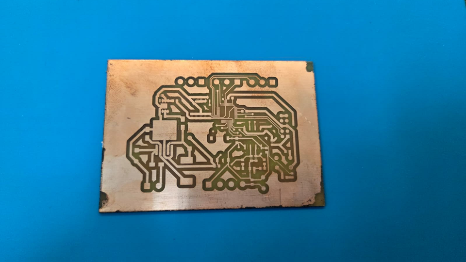
Final drilled and milled PCB result photo:
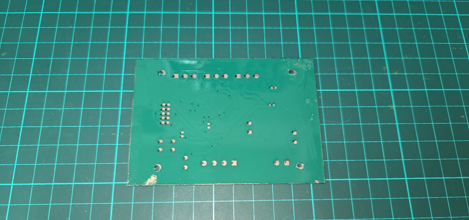
Step 13: The PCB Mask and Laser Processing
We prepare the surface of the PCB by lightly using a high grid sandpaper, and then isopropyl alcohol. We have applied the green mask.
Use the Snapmaker Laser module again (with the solder mask G-code generated earlier) to ablate the paint only over the pads, exposing them for soldering.
While removing the mask:

Remember, we can use the laser module machine coordinates for our work origin.
Here are the results:

And for the bottom copper:
Notice that the vias are slightly offset from the pads. While not perfect, this is manageable for a prototype. You can fix most of these by feeding in extra solder to bridge the gap or, in extreme cases, running a tiny jumper wire to the adjacent trace. Don’t let a minor offset stop your workflow—patch it up and keep testing!
Step 14: Cutting and Finishing
Cutting
We go back to the CNC module by swapping the modules.
Now, we can run our final G-code and remember, we can use the CNC machine coordinates for the work origin. From that point, we cut our PCB:

Then we got the cut PCB,

Sanding
Now, we sand the edges,

Final Result
Finally, we have our PCBs!

Bottom copper:


Ahmet Batuhan Günaltay is a final-year Electrical and Electronics Engineering student at Dokuz Eylül University and a veteran of Solar Team Solaris.
Check on LinkedIn